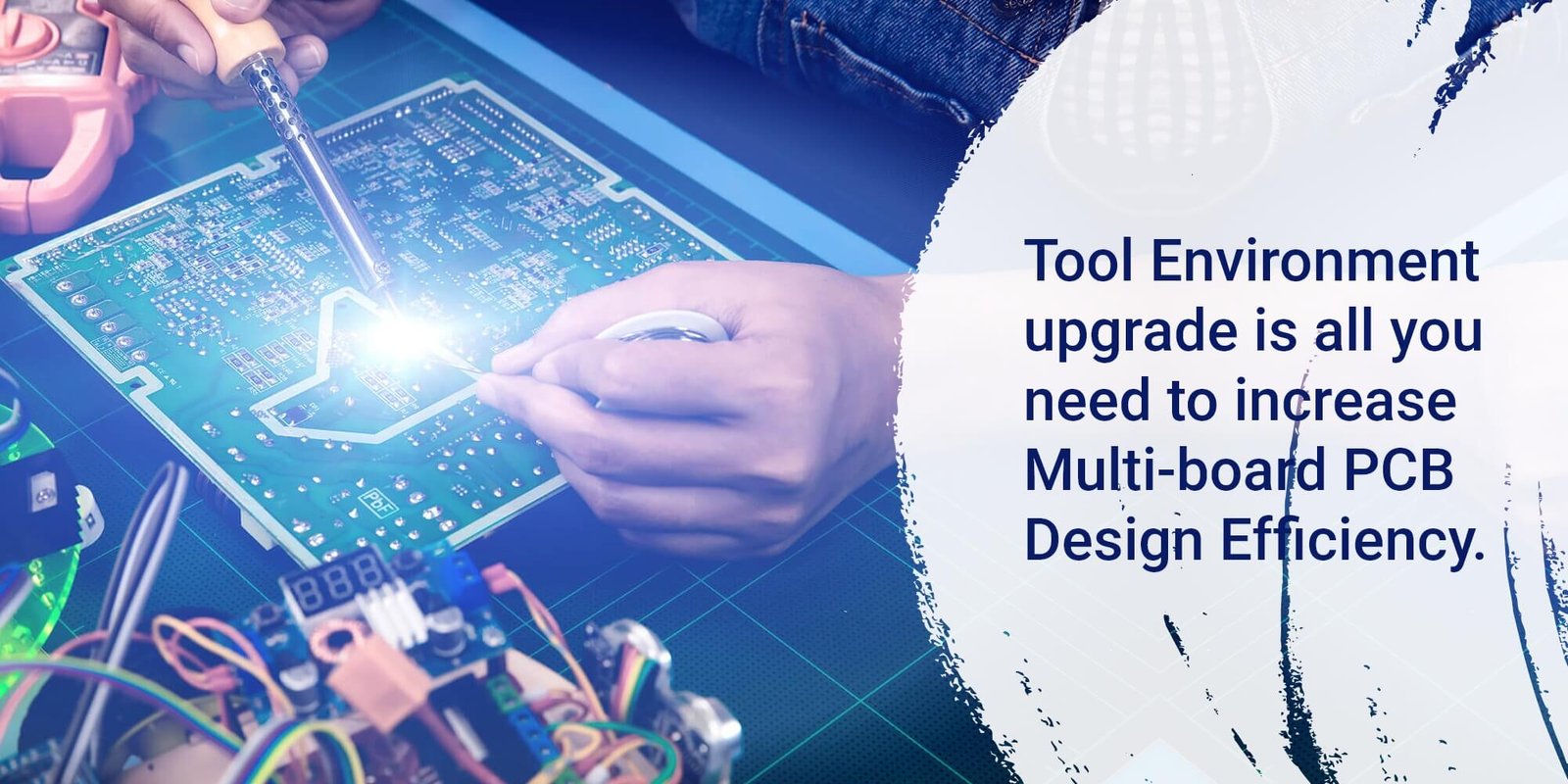
Tool Environment upgrade is all you need to increase Multi-board PCB Design Efficiency.
- If you open some of your favorite electronics, you will find a multi-board system or some PCBs connected along with cables and ribbons. To deal with older PCB circuits, you will have to refactor them. The approach had not been systematic, and the design was not safely built. Avoiding mistakes can become a big mistake while designing a circuit.
Design platforms have paved the way for certain aspects of varied circuit board designers. But the choice of an appropriate design matters. This, in turn, can lead to the making of an exceptional quality PCB board. Thus, the design board gets approved. Building a print circuit board is considered a difficult task. Translating device requirements into work circuits that supply the necessary functionality involves many design decisions. The designer must balance the PCB requirements, colliding perfectly with the basic needs of the same. This is the central puzzle that must be united by the developer carefully, and fortunately, PCB designers have become excellent puzzle breakers.
A new puzzle has appeared with a system design of several PCBs; it’s just not so much “piece” Because this is an entirely new puzzle. System design involves many participants and tools but now becomes more work than PCB designers. The idea is great for building a Board, but summing up the parts again becomes difficult for the designers. With the ongoing Multi-Board PCB design process analysis, developers can offer several insights into setting a workflow that is useful for system design.
Table of Contents
Overview, The Multi-Board PCB Design Process, formats with good information
Landscape design and electronic technology shift encourage more imaginative engineering solutions, faster, more efficient, flexible, and easy to learn. Grasping knowledge on PCB design is not a single day’s work. It will need various weeks with serious dedication. Now you work with all system boards, the need for complete information is even more significant. For example, will the board be produced together in the same panel while in the PCB Assembly phase? If so, then you must plan their stack-up layer accordingly.
You don’t only need to work with all your design team members to ensure that software and mechanical requirements are clearly expressed but also with your manufacturer. The multi-board design aims to reduce various enhancement methods of time by forming one of the best-accredited designs across the globe. The last factor you want is to slow down the pace of your multi-board design process with a single board design practice and procedure.
Parts of PCB requiring tool upgradation
- Statue part
Placing all the elements in the correct locations is essential. Vital factors like plug personalization and board alignment need to be kept in mind. The statue part is stationary, and the Board’s ethics are maintained with ease.
- Important parts
Microprocessors, memory chips, power supply, or other board main components are usually the next part placed.
- Support section
The power supply component will have an additional part associated with it and microprocessors and memory devices.
- The remaining part
The left-out parts are considered as “not so important.” But this is not the fact. It is an extended idea of developing certain vertical placements so that the board doesn’t get corroded.

Tool environment upgrade needs to increase Multi-board PCB Design Efficiency
PCB layout or ethical design is a vital and strong point. After all the work has been done, components and their allotment to their specific parts are checked for safety purposes. Component information from schematic symbols and net connectivity need to be converted by the designer into the required data for the PCB layout.
- Library section
Model physical components, such as resistors, need to be made in layout accessories. Such models are often known as footprints or soil patterns and will contain a metal pad representation which will ultimately solder the component pin. They will also have certain forms of electrical components and data, fasteners, and 3D.
- Design rules
Many engineers fail to study the diagram of a PCB board. The diagnostic approach via code is ignored, but the solution to this has been made available. The PCB design CAD tool has a broad rule and system constraints built into it to regulate the size and distance of metal objects. These rules must be fully controlled or copied from the previous design before the layout starts.
- Outline
Physical form and circuit board structure also need to be set in the layout database. The CAD system will automatically enhance and suggest prolific ideas for a proper design outlook. Outlining the parts again becomes an easier time. Thus, we can say that the blueprint of a PCB board makes the work easier.
Multi-board system-level design needs
Historically, the PCB design has been handled by the Board. Age-old techniques need to be avoided since the PCB board is an advanced form and an integral part of all the electronic elements. This is standard practice, but more extended design systems cannot develop a multi-board to start. After the PCB design prototype is built, the board will be tested for forms, fitting, and functioning with other system boards.
This approach no longer serves the advanced technology that is being made today. Requirements for more system-level design increase while the need to shorten the design cycle is increasing too. The builder must regulate traditional PCB design systems with CAD tools that can handle multi-board system-level design complexity.
Set your design rules
Some of each PCB layout is preparing design parameters and rules and obstacles from design. With a multi-board circuit, several touches need to be formed to every structure present on the elemental view. All the components, parts of the PCB library parts, stack-up layers, and formation rules will brief the designer.
San Diego, Ca. Altium LLC interpreted the problems and gave rise to the Altium Designer 18 tool to better manifest the ideas while building a PCB. This version upgrade focuses on increasing user experience by updating the main features and improvements that focus on the productivity available in one modern design ecosystem, easy to use. The software is surely going to rule the PCB world for a long time. The designer kits and accessories available make it further access to all the builders of PCB boards. Altium keeps up its motto to focus on developing the latest upgraded facilities of the accessories for easier access by the current engineers.